 |

|
| ActiveWin: Reviews | Active Network | New Reviews | Old Reviews | Interviews |Mailing List | Forums |
|
|
|
|
|
DirectX |
|
ActiveMac |
|
Downloads |
|
Forums |
|
Interviews |
|
News |
|
MS Games & Hardware |
|
Reviews |
|
Support Center |
|
Windows 2000 |
|
Windows Me |
|
Windows Server 2003 |
|
Windows Vista |
|
Windows XP |
|
|
|
|
|
|
|
News Centers |
|
Windows/Microsoft |
|
DVD |
|
Apple/Mac |
|
Xbox |
|
News Search |
|
|
|
|
|
|
|
ActiveXBox |
|
Xbox News |
|
Box Shots |
|
Inside The Xbox |
|
Released Titles |
|
Announced Titles |
|
Screenshots/Videos |
|
History Of The Xbox |
|
Links |
|
Forum |
|
FAQ |
|
|
|
|
|
|
|
Windows XP |
|
Introduction |
|
System Requirements |
|
Home Features |
|
Pro Features |
|
Upgrade Checklists |
|
History |
|
FAQ |
|
Links |
|
TopTechTips |
|
|
|
|
|
|
|
FAQ's |
|
Windows Vista |
|
Windows 98/98 SE |
|
Windows 2000 |
|
Windows Me |
|
Windows Server 2002 |
|
Windows "Whistler" XP |
|
Windows CE |
|
Internet Explorer 6 |
|
Internet Explorer 5 |
|
Xbox |
|
Xbox 360 |
|
DirectX |
|
DVD's |
|
|
|
|
|
|
|
TopTechTips |
|
Registry Tips |
|
Windows 95/98 |
|
Windows 2000 |
|
Internet Explorer 5 |
|
Program Tips |
|
Easter Eggs |
|
Hardware |
|
DVD |
|
|
|
|
|
|
|
ActiveDVD |
|
DVD News |
|
DVD Forum |
|
Glossary |
|
Tips |
|
Articles |
|
Reviews |
|
News Archive |
|
Links |
|
Drivers |
|
|
|
|
|
|
|
Latest Reviews |
|
Xbox/Games |
|
Fallout 3 |
|
|
|
Applications |
|
Windows Server 2008 R2 |
|
Windows 7 |
|
|
|
Hardware |
|
iPod Touch 32GB |
|
|
|
|
|
|
|
Latest Interviews |
|
Steve Ballmer |
|
Jim Allchin |
|
|
|
|
|
|
|
Site News/Info |
|
About This Site |
|
Affiliates |
|
Contact Us |
|
Default Home Page |
|
Link To Us |
|
Links |
|
News Archive |
|
Site Search |
|
Awards |
|
|
|
|
|
|
|
Credits |

|
Product: Pentium 4 2.8GHz & Intel D845EBT
Motherboard |
New SSE2 Instruction Set
| Table Of Contents |
| 1:
Introduction 2: CPU Architecture 3: SSE2 Instructions & P4 2.8GHz CPU Design 4: Intel i82845e Chipset 5: Intel D845EBT Motherboard 6: Intel D845EBT Sound Features 7: Synthetic Benchmarks 8: Games Benchmarks 9: Applications Benchmarks 10: Benchmarks analysis 11: Conclusion |
Intel introduced the MMX (MMX for MultiMedia eXtensions) instructions set
back in
The SSE
instruction set principally enhances audio and video compression processes
as shown by our tests: indeed compressing an audio file of
Thermal Security
The Pentium
Pentium 4 2.8GHz CPU Design
The Pentium 4 2.8 GHz uses the µPGA Socket

Intel Pentium 4 2.8GHz
After
having changed the packaging of Pentium

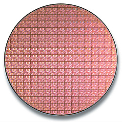
Pentium 4 0.13µ Wafer (click
to enlarge)
Since the
engraving process is finer and more accurate there’s more room available on
the silica plaque so Intel engineers have increased the level
As usual
the top part of the CPU features a metal cover that was added by Intel to
protect the die unit from damage if the radiator was incorrectly mounted or
is too heavy as well as to ensure better thermal dissipation. The heat sink
has been totally revamped. Intel has released a new plastic retention
mechanism (which is much handier) to attach the cooler and heat sink to the
motherboard. Nonetheless you can still use old school Pentium

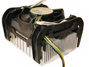
Pentium 4 Heatsink with
retention mechanism (click to enlarge)
Actually
the Pentium
