The Active Network
ActiveWin: Reviews Active Network | New Reviews | Old Reviews | Interviews |Mailing List | Forums 
 

Amazon.com

  *  


Product: Pentium 4 2.8GHz & Intel D845EBT Motherboard
Company: Intel
Website: http://www.intel.com
Estimated Street Price:
$637
Review By: Julien Jay

CPU Architecture

Table Of Contents
1: Introduction
2: CPU Architecture
3: SSE2 Instructions & P4 2.8GHz CPU Design
4: Intel i82845e Chipset
5: Intel D845EBT Motherboard
6: Intel D845EBT Sound Features
7: Synthetic Benchmarks
8: Games Benchmarks
9: Applications Benchmarks
10: Benchmarks analysis
11:
Conclusion

Note: If you have already read our previous Pentium 4 reviews, you can skip this technical part and directly jump to the ‘A New Bus: Don't Misse It’ chapter.

   This gets complicated! Built on a P7 core engine, the Pentium 4 is the first processor from the brand new IA-32 NetBurst micro-architecture that allows operating at higher performance levels and clock speeds when compared to previous IA-32 based processors. The NetBurst architecture really boosts performance but don’t think that it’ll boost Internet download time, transfer rate, etc. The name of the architecture has no link with the Internet. With the NetBurst architecture Pentium 4 processors promise to support without any problem a several Gigahertz clock speed without the need for Intel to make major changes in its manufacturing process. The NetBurst architecture is also the first one to use a 20 stage pipeline against only 10 for the Pentium III and that can store up to 126 instructions –in flight-. A pipeline is a group of units that achieve to work together hand-in-hand in order to handle software instructions. With more pipelines, tasks are managed in a shorter time and require fewer transistors than before, allowing higher frequency operation.  

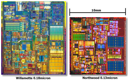
Intel Pentium 4 Willamette & Northwood Dies

Even though using more pipelines present several advantages it has also a major drawback: to handle the software instructions the processor tries to guess which one will be the next using tests. With a pipeline enabled CPU the instructions that follow the test should be managed before the processor knows the test result in order to continually feed the pipeline. To know which instructions should be used the CPU uses a ‘branch prediction’ mechanism: most of the time the CPU runs instructions it has already ran before and probably knows the result ahead of time. It has a 4x larger BTB (branch target buffer) than on the Pentium III to store the history of all previous tests results in 4 KB of memory which helps software to make decisions. If the CPU encounters a test that has already run it’ll use the same branch as before in order to accelerate its work speed. Pentium 4 processors achieve more than 94% of successful predictions (against only 90% for a Pentium III which Intel claims to be a gain of 33%). 

 But in case of a test failure the whole BTB is trashed as well as all the pipelines in order for the CPU to restart the operation: this process obviously slows down the whole performance of the computer. The Pentium 4 CPU also takes charge of ‘out of order’ instructions in order to not block ALU processes unlike when they are run in ordered mode. Like with every P6 based processor the Pentium 4 comes with two arithmetic logic units and one floating point unit known as superscalar architecture (Pentium CPUs were the first to use it). NetBurst architecture brings a major enhancement known as the Rapid Execution Engine to the superscalar architecture since both the ALU (Arithmetic Logic Unit) & the AGU (Address Generation Unit that manages where data are stored and loaded in the correct address) work twice as fast as the CPU frequency, so it can now handle four instructions per cycle rather than two before. For example, the Rapid Execution Engine on a 2.8 GHz Intel Pentium 4 processor runs at 5.6 GHz.

For those of you who don’t know an ALU is the name that was given to the integer unit that manages math related operations like dividing, adding, multiplying as well as logical operators like ‘OR’, ‘AND’, ‘XOR’, etc. Just like every good superscalar processor worth of this name, the Pentium 4 still includes a ‘Micro Operation Operand’ Unit that comes with simple instructions directly managed by the processor: most of the time x86 instructions are converted into Ops.  


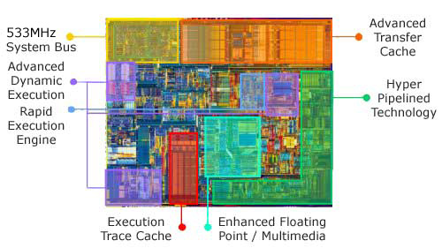
Intel Pentium 4 Architecture Schema

With the 486 DX4 and the Pentium, Intel introduced on board cache memory directly in the chip: it was a premiere that boosted performance. Pentium III enhanced further this concept by integrating on-die cache memory. The Pentium 4 cache memory characteristic has also evolved: L1 cache memory now includes a 8 KB data cache (which is quite small when you know the PIII included a 32KB one) while the L1 Instruction Cache was renamed to Instruction Trace Cache since it has widely evolved too. The Pentium 4 L1 cache uses a four way set and uses 64 byte cache lines and due to its dual port design it can store data while loading it. Trace Cache memory now stores instructions after they are converted from x86 into micro-ops in the order they should be run, saving processor cycles if a bad branch prediction occurs (since the alternative solution is already stored in it). This also allows faster access to the most used instructions avoiding problems Pentium III may have with complex x86 instructions that were decoded with slow decoders.  

Trace Cache memory can store 12,000 micro-ops which corresponds to an approximate size of 92 or 96 KB (Intel didn’t specify the exact size). Once µOPs are in the trace cache, the Pentium 4 can easily check for dependencies to correctly achieve its branch predictions and ensure that the pipelines are continuously supplied with data: the trace cache can contains a whole pipeline with 6 µOps each 2 clocks. The L1 cache access speed is now about 1.4 nano seconds (twice as fast as Pentium III) and the bandwidth now reaches 41.7 GB/s (against 14.9GB/s for a Pentium III). L2 memory cache has also been enhanced. The level 2 cache memory amount now reaches 512 KB and runs at the full frequency speed of the CPU (and not like on Pentium II or first Pentium III at a twice-slower speed than the nominal frequency of the CPU).  

As a reminder Level 2 cache memory enhances computer performance by approximately 20%. L2 Pentium 4 on die cache memory bandwidth now reaches 81 GB per second for a Pentium 4 2.53 GHz, since it uses 128 bytes cache lines divided in two 64 bytes pieces reading at least 64 bytes of data in one pass, ensuring highest performance. This compares to a transfer rate of 16 GB/s on the Pentium III processor at 1 GHz.

A new Bus: Don't Miss It

   Over the months, the 400 MHz FSB of the Pentium 4 has somewhat become a bottleneck with the recent CPU frequency increase we have seen. Even if a 400 MHz FSB was sufficient for a 1.5 GHz P4, it is clearly limited for 2.0 GHz and faster CPUs. That’s why Intel engineers have boosted the front side bus of the Pentium 4 to 533 MHz.  

The Pentium 4 now comes with a 533 MHz front side bus using a Quad Pumped 64-bit bus where each level operates at 133 MHz for a global 4.2 GB/s bandwidth representing a 33.3% increase of the processor bus bandwidth. Intel used a technical trick so the FSB sends four 64-bit instructions per cycle making it work like a “533 MHz” normal one. Not only does this bus improve performance but it’s also the first one that lets an x86 processor exchange data so fast between the CPU, the memory and the rest of the system components. To achieve full performance a processor with a 533 MHz FSB should be teamed up with new Rambus 1066 memory.

« Introduction SSE2 Instructions & P4 2.8GHz CPU Design »


  *  
  *   *