 |

|
| ActiveWin: Reviews | Active Network | New Reviews | Old Reviews | Interviews |Mailing List | Forums |
|
|
|
|
|
DirectX |
|
ActiveMac |
|
Downloads |
|
Forums |
|
Interviews |
|
News |
|
MS Games & Hardware |
|
Reviews |
|
Support Center |
|
Windows 2000 |
|
Windows Me |
|
Windows Server 2003 |
|
Windows Vista |
|
Windows XP |
|
|
|
|
|
|
|
News Centers |
|
Windows/Microsoft |
|
DVD |
|
Apple/Mac |
|
Xbox |
|
News Search |
|
|
|
|
|
|
|
ActiveXBox |
|
Xbox News |
|
Box Shots |
|
Inside The Xbox |
|
Released Titles |
|
Announced Titles |
|
Screenshots/Videos |
|
History Of The Xbox |
|
Links |
|
Forum |
|
FAQ |
|
|
|
|
|
|
|
Windows XP |
|
Introduction |
|
System Requirements |
|
Home Features |
|
Pro Features |
|
Upgrade Checklists |
|
History |
|
FAQ |
|
Links |
|
TopTechTips |
|
|
|
|
|
|
|
FAQ's |
|
Windows Vista |
|
Windows 98/98 SE |
|
Windows 2000 |
|
Windows Me |
|
Windows Server 2002 |
|
Windows "Whistler" XP |
|
Windows CE |
|
Internet Explorer 6 |
|
Internet Explorer 5 |
|
Xbox |
|
Xbox 360 |
|
DirectX |
|
DVD's |
|
|
|
|
|
|
|
TopTechTips |
|
Registry Tips |
|
Windows 95/98 |
|
Windows 2000 |
|
Internet Explorer 5 |
|
Program Tips |
|
Easter Eggs |
|
Hardware |
|
DVD |
|
|
|
|
|
|
|
ActiveDVD |
|
DVD News |
|
DVD Forum |
|
Glossary |
|
Tips |
|
Articles |
|
Reviews |
|
News Archive |
|
Links |
|
Drivers |
|
|
|
|
|
|
|
Latest Reviews |
|
Xbox/Games |
|
Fallout 3 |
|
|
|
Applications |
|
Windows Server 2008 R2 |
|
Windows 7 |
|
|
|
Hardware |
|
iPod Touch 32GB |
|
|
|
|
|
|
|
Latest Interviews |
|
Steve Ballmer |
|
Jim Allchin |
|
|
|
|
|
|
|
Site News/Info |
|
About This Site |
|
Affiliates |
|
Contact Us |
|
Default Home Page |
|
Link To Us |
|
Links |
|
News Archive |
|
Site Search |
|
Awards |
|
|
|
|
|
|
|
Credits |

|
Product: Intel Pentium 4 1.7GHz & Intel
D850GB MotherBoard |
CPU Architecture
|
Table Of Contents |
This gets complicated! Built on a P6 core engine, the Pentium 4 is the first processor from the brand new IA-32 NetBurst micro-architecture that allows operating at higher performance levels and clock speeds when compared to previous IA-32 based processors. The NetBurst architecture really boosts performance but don’t think that it’ll boost your internet downloading times, transfer rate, etc. The name of the architecture has no link with the Internet. With the NetBurst architecture, Pentium 4 processors promise to support without any problem a several Gigahertz clock speeds without the need for Intel to make major changes in its manufacturing process.


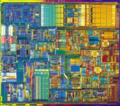
Intel Pentium 4 Die
| Review Quotes | ||||
| "NetBurst architecture brings a major enhancement known as the Rapid Execution Engine to the superscalar architecture " | ||||
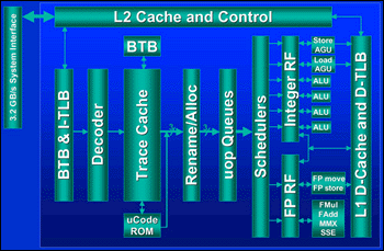
The NetBurst architecture is also the first one to use a 20 stage pipeline against only 10 for the Pentium III, that can stores up to 126 instructions –in flight-. A pipeline is a group of units that achieve to work together hand-in-hand in order to handle software instructions. With more pipelines, tasks are managed in a shorter time and require fewer transistors than before, allowing higher frequency operation. If using more pipelines present several advantages it has also a major drawback: to handle the software instructions the processor tries to guess which one will be the next using tests. With a pipeline enabled CPU the instructions that follow the test should be managed before the processor knows the test result in order to continually feed the pipeline. To know which instructions should be used the CPU uses a ‘branch prediction’ mechanism: most of the time the CPU runs instructions it has already ran before and probably knows the result ahead of time. It has a four times larger BTB (branch target buffer) than on the Pentium III to store the history of all previous tests results in 4KB of memory which helps software to make decisions. If the CPU encounters a test that has already run it’ll use the same branch as before in order to accelerate its work speed. Pentium 4 processors achieve more than 94% of successful predictions (against only 90% for a Pentium III which Intel claims to be a gain of 33%). But in case of a test failure the whole BTB is trashed as well as all the pipelines in order for the CPU to restart the operation: this process obviously slows down the whole performance of the computer. The Pentium 4 CPU also takes charge of ‘out of order’ instructions in order to not block ALU processes unlike when they are run in ordered mode. Like with every P6 based processor the Pentium 4 comes with two arithmetic logic units and one floating point unit known as superscalar architecture (Pentium CPUs were the first to use it). NetBurst architecture brings a major enhancement known as the Rapid Execution Engine to the superscalar architecture since both the ALU (Arithmetic Logic Unit) & the AGU (Address Generation Unit that manages where data are stored and loaded in the correct address) work twice as fast as the CPU frequency, so it can now handle four instructions per cycle rather than two before. For those of you who don’t know an ALU is the name that was given to the integer unit that manages math related operations like dividing, adding, multiplying as well as logical operators like ‘OR’, ‘AND’, ‘XOR’, etc. Just like every good superscalar processor worth of this name, the Pentium 4 still includes a ‘Micro Operation Operand’ Unit that comes with simple instructions directly managed by the processor: most of the time x86 instructions are converted into Ops.

Intel Pentium 4 Architecture Schema
With the 486 DX4 and the Pentium, Intel introduced on board
cache memory directly in the chip: it was a premiere that boosted
performance. Pentium III enhanced further this concept by integrating
on-die cache memory. So the Pentium 4 cache memory characteristic have
also evolved: L1 cache memory now includes a 8 KB data cache (which is
quite small when you know the PIII included a 32KB one) while the L1
Instruction Cache was renamed to Instruction Trace Cache since it has
widely evolved too. The Pentium 4 L1 cache uses a four way set and uses 64
byte cache lines and due to its dual port design it can store data while
loading it. Trace Cache memory now stores instructions after they are
converted from x86 into micro-ops in the order they should be run, saving
processor cycles if a bad branch prediction occurs (since the alternative
solution is already stored in it). This also allows faster access to the
most used instructions avoiding problems Pentium III may have with complex
x86 instructions that were decoded with slow decoders. Trace Cache memory
can stores 12,000 micro-ops which corresponds to an approximate size of 92
or 96 KB (Intel didn’t specify the exact size). Once µOPs are in the trace
cache the Pentium 4 can easily check for dependencies to correctly achieve
its branch predictions and ensure that the pipelines are continuously
supplied with data: the trace cache can contains a whole pipeline with 6
µOps each 2 clocks. The L1 cache access speed is now about 1.4 nano
seconds (twice as fast as Pentium III) and the bandwidth now reaches
41.7GB/s (against 14.9 for a Pentium III). L2 memory cache has also been
enhanced. Like on the Coppermine CPU, if the level 2 cache memory amount
reaches 256KB it runs at the full frequency speed of the CPU (and not like
on Pentium II or first Pentium III at a twice-slower speed than the
nominal frequency of the CPU). As a reminder Level 2 cache memory enhances
computer brut performance by approximately 25%. L2 Pentium 4 on die cache
memory bandwidth now reaches the incredible amount
of 54.4 GB per second for
this 1.7
GHz model (against 48GB per second for the 1.5GHz),
since it uses 128 bytes cache lines divided in two 64 bytes pieces reading
at least 64 bytes of data in one pass, ensuring highest performance.

Intel Pentium 4 1.7GHz
To draw a perfect picture of the Pentium 4 we shouldn’t forget to say that it includes a micro-code ROM allowing users to upload new micro code ROMs in order to solve minor problems.
A new Bus don't miss it!
| Review Quotes | ||||
| "Pentium 4 Bus exchanges data with the rest of the system faster than ever removing one of the major bottleneck Pentium III had " | ||||
Latest Pentium III processors use a 133Mhz –only- front side bus with a 1065Mbps bandwidth, that was a bit pale compared to the AMD Athlon ‘266’ one. The front side bus has always been a real strangulation for a high performance PC. With 400 MHz computer a FSB of 100 MHz was just sufficient but for a 1 GHz plus computer a 133 MHz was a bit weak. Intel has revamped it by introducing a 400 MHz front side bus using a Quad Pumped 64-bit bus where each level operates at 100 MHz for a global 3051 MB/s bandwidth. Intel used a technical trick so the FSB sends four 64-bit instructions per cycle making it work like a “400 MHz” normal one. Not only this new bus improves performances but it’s also the first one that lets an x86 processor exchanges data so fast between the CPU, the memory and the rest of the system components - leaving far behind the recent AMD EV6-bus.

Pentium 4 Golden Pegs
