 |

|
| ActiveWin: Reviews | Active Network | New Reviews | Old Reviews | Interviews |Mailing List | Forums |
|
|
|
|
|
DirectX |
|
ActiveMac |
|
Downloads |
|
Forums |
|
Interviews |
|
News |
|
MS Games & Hardware |
|
Reviews |
|
Support Center |
|
Windows 2000 |
|
Windows Me |
|
Windows Server 2003 |
|
Windows Vista |
|
Windows XP |
|
|
|
|
|
|
|
News Centers |
|
Windows/Microsoft |
|
DVD |
|
Apple/Mac |
|
Xbox |
|
News Search |
|
|
|
|
|
|
|
ActiveXBox |
|
Xbox News |
|
Box Shots |
|
Inside The Xbox |
|
Released Titles |
|
Announced Titles |
|
Screenshots/Videos |
|
History Of The Xbox |
|
Links |
|
Forum |
|
FAQ |
|
|
|
|
|
|
|
Windows XP |
|
Introduction |
|
System Requirements |
|
Home Features |
|
Pro Features |
|
Upgrade Checklists |
|
History |
|
FAQ |
|
Links |
|
TopTechTips |
|
|
|
|
|
|
|
FAQ's |
|
Windows Vista |
|
Windows 98/98 SE |
|
Windows 2000 |
|
Windows Me |
|
Windows Server 2002 |
|
Windows "Whistler" XP |
|
Windows CE |
|
Internet Explorer 6 |
|
Internet Explorer 5 |
|
Xbox |
|
Xbox 360 |
|
DirectX |
|
DVD's |
|
|
|
|
|
|
|
TopTechTips |
|
Registry Tips |
|
Windows 95/98 |
|
Windows 2000 |
|
Internet Explorer 5 |
|
Program Tips |
|
Easter Eggs |
|
Hardware |
|
DVD |
|
|
|
|
|
|
|
ActiveDVD |
|
DVD News |
|
DVD Forum |
|
Glossary |
|
Tips |
|
Articles |
|
Reviews |
|
News Archive |
|
Links |
|
Drivers |
|
|
|
|
|
|
|
Latest Reviews |
|
Xbox/Games |
|
Fallout 3 |
|
|
|
Applications |
|
Windows Server 2008 R2 |
|
Windows 7 |
|
|
|
Hardware |
|
iPod Touch 32GB |
|
|
|
|
|
|
|
Latest Interviews |
|
Steve Ballmer |
|
Jim Allchin |
|
|
|
|
|
|
|
Site News/Info |
|
About This Site |
|
Affiliates |
|
Contact Us |
|
Default Home Page |
|
Link To Us |
|
Links |
|
News Archive |
|
Site Search |
|
Awards |
|
|
|
|
|
|
|
Credits |

|
Product: Intel D815EPEA2 & Celeron
850/100MHz Review |
Celeron 850MHz
|
Table Of Contents |
 When
the Celeron was launched in early 1998, this new processor positioned
itself as an alternative to the Pentium II offering more power than Intel
Pentium MMX processors at an affordable price. However the first Celeron
were really too bridled. Indeed there wasn’t any second level cache memory
on first 266MHz & 300MHz models resulting in average performance. Even
with this limitation the processor was a best seller and acclaimed by most
users because it was very easily overclockable. Intel has made this little
processor evolve over the years into a mature alternative for affordable
but powerful PCs, by adding a welcome 128 KB second level cache memory and
more recently a long desired 100MHz frontside bus to boost performance as
well as some other neat enhancements. In fact, some people call the
Celeron 850/100 CPU we have reviewed a Celeron 2. This new Celeron from
Intel is in fact a light version of Coppermine series of CPUs that uses
the P6 micro architecture: The Celeron 850MHz now shares the same SSE
instructions set than the Pentium III, uses a 100MHz FSB, is equipped with
128 KB of second level cache memory, is now engraved using 0,18µ
technology and comes in a FC-PGA Socket 370 Form Factor. This new FC-PGA
format is supposed to be more adapted to high frequencies today processors
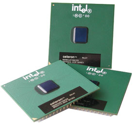
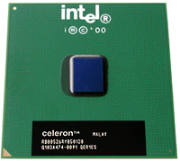
offer. Pentium III and Celeron CPUs now look exactly the same, only the markings differ.
During our tests the
Celeron 850MHz didn’t heat a lot: it only reach the
maximum temperature of 87.8 F (31.0° Celsius) after
intensive use, demonstrating good resistance when users overclock
it.

Various Intel Processors
(click to enlarge)

Intel Celeron 850MHz (click
to enlarge)
Thanks to the 0,18µ technology the Celeron heats less than before and so its voltage has been changed from 2 to 1.6 volts. The Celeron 850MHz fully supports MMX extensions: Intel MMX technology includes instructions and data types that allow applications to achieve a new level of performance. Intel’s MMX technology is designed as a set of basic, general-purpose integer instructions that are easily applied to the needs of a wide diversity of multimedia and communications applications. The highlights of the technology are: Single Instruction, Multiple Data (SIMD) technique, 57 new instructions, Eight 64-bit wide MMX technology registers, and four new data types. Adding SSE instructions to the Celeron 2 is a good thing since those instructions will complete the MMX ones to boost some operations with games or applications that use the Direct X APIs from Microsoft. SSE instructions are especially dedicated to enhanced overall 3D performance. The Internet Streaming SIMD Extensions consist of 70 new instructions (with 52 Floating point ones) and includes single instruction, multiple data for floating-point, additional SIMD-integer and Cacheability control instructions. In comparison to casual SISD (single instruction, single date) the SIMD instructions of the MMX & SSE set of instructions can work on several data types at the same time (up to 4 floating numbers in 32bits for SSE). Some of the benefits to desktop and Internet applications of Internet Streaming SIMD Extensions include: higher resolution and quality images can be viewed and manipulated than previously possible, high quality audio, MPEG2 video, and simultaneous MPEG2 encoding and decoding, reduced CPU utilization for speech recognition, as well as higher accuracy and faster response times.
One thing is very important in the architecture of every processor: the cache memory. For memory, the cache memory stores the most used instructions or data to speed up operations and reduces computing delays. The Celeron 850MHz comes with 16KB of data and another 16 KB instructions L1 cache. The L1 cache memory ensures that the CPU is always fed with data so it really has a significant impact on performance. Also included with the Celeron 850MHz is an on-die 128KB 4 way associative L2 cache (against 256Kb 8 way associative for Pentium III) clocked at the CPU full speed that is to say 850 MHz and connected to it through a 256-bit bus. First Celeron used a 64 bit only bus so this new 256-bit bus can convey more data in one single clock cycle resulting in better performances, once again.
