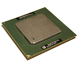
 |

|
| ActiveWin: Reviews | Active Network | New Reviews | Old Reviews | Interviews |Mailing List | Forums |
|
|
|
|
|
DirectX |
|
ActiveMac |
|
Downloads |
|
Forums |
|
Interviews |
|
News |
|
MS Games & Hardware |
|
Reviews |
|
Support Center |
|
Windows 2000 |
|
Windows Me |
|
Windows Server 2003 |
|
Windows Vista |
|
Windows XP |
|
|
|
|
|
|
|
News Centers |
|
Windows/Microsoft |
|
DVD |
|
Apple/Mac |
|
Xbox |
|
News Search |
|
|
|
|
|
|
|
ActiveXBox |
|
Xbox News |
|
Box Shots |
|
Inside The Xbox |
|
Released Titles |
|
Announced Titles |
|
Screenshots/Videos |
|
History Of The Xbox |
|
Links |
|
Forum |
|
FAQ |
|
|
|
|
|
|
|
Windows XP |
|
Introduction |
|
System Requirements |
|
Home Features |
|
Pro Features |
|
Upgrade Checklists |
|
History |
|
FAQ |
|
Links |
|
TopTechTips |
|
|
|
|
|
|
|
FAQ's |
|
Windows Vista |
|
Windows 98/98 SE |
|
Windows 2000 |
|
Windows Me |
|
Windows Server 2002 |
|
Windows "Whistler" XP |
|
Windows CE |
|
Internet Explorer 6 |
|
Internet Explorer 5 |
|
Xbox |
|
Xbox 360 |
|
DirectX |
|
DVD's |
|
|
|
|
|
|
|
TopTechTips |
|
Registry Tips |
|
Windows 95/98 |
|
Windows 2000 |
|
Internet Explorer 5 |
|
Program Tips |
|
Easter Eggs |
|
Hardware |
|
DVD |
|
|
|
|
|
|
|
ActiveDVD |
|
DVD News |
|
DVD Forum |
|
Glossary |
|
Tips |
|
Articles |
|
Reviews |
|
News Archive |
|
Links |
|
Drivers |
|
|
|
|
|
|
|
Latest Reviews |
|
Xbox/Games |
|
Fallout 3 |
|
|
|
Applications |
|
Windows Server 2008 R2 |
|
Windows 7 |
|
|
|
Hardware |
|
iPod Touch 32GB |
|
|
|
|
|
|
|
Latest Interviews |
|
Steve Ballmer |
|
Jim Allchin |
|
|
|
|
|
|
|
Site News/Info |
|
About This Site |
|
Affiliates |
|
Contact Us |
|
Default Home Page |
|
Link To Us |
|
Links |
|
News Archive |
|
Site Search |
|
Awards |
|
|
|
|
|
|
|
Credits |


|
Product: Pentium 4 2.2GHz - Intel D845BG
Motherboards Company: Intel Website: http://www.intel.com Estimated Street Price: $529.00 (for the CPU) Review By: Julien Jay |
Intel Celeron 1.3GHz CPU Design
|
Table Of Contents |

Intel’s plan to eradicate the Pentium III is based on two axes: making the Pentium 4 affordable while offering entry level processors that match the level of performance offered by the Pentium III. The recently released Celeron 1.3GHz is part of this plan.
Previous Celeron CPUs (800/850/900MHz, etc.) have in common with the Pentium III family the same Coppermine core. Despite a common core, they featured a few differences: Celeron offered a slow 128Kb on-die cache (against 256Kb for the PIII) with a FSB clocked at 100MHz (against 133MHz for the Pentium III).
The new Celeron 1.3GHz is surprising at many levels! Indeed it’s now strictly identical to a Tualatin CPU apart for the FSB that is still stuck at 100MHz. The Celeron 1.3 GHz offers a new 256KB, 8 ways associative, full speed, on die cache memory. Intel Celeron 1.3GHz uses the FC-PGA2 package to fit in Socket 370 slots: so you’ll find a IHS (Integrated Heat Spreader) metal cover protecting the CPU’s core and ensuring a better thermal dissipation. The CPU obviously supports MMX and SSE instructions including a Data Prefetch to automatically pre-load data into the L2 cache memory.
Due to the fact this high end Celeron uses the Tualatin core it requires a motherboard using the revision B of the Intel 815 chipset. Indeed CPUs based on the Tualatin core now come with 10 supplementary pins, use the AGTL bus, consume 1.25 volts (against 1.5volts for previous PIII/Celerons) and use revision 8.5 of the VRM (Voltage Regulator Module).
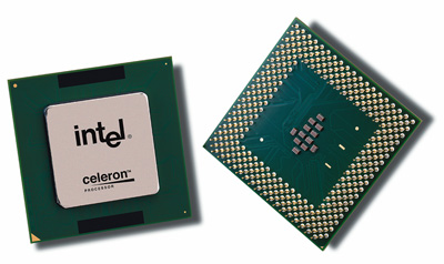
Intel Celeron (click to
enlarge)
Pentium III (aka Tualatin) 1.2GHz CPU Design

The latest representative of the Intel Pentium III family has been released for awhile and is officially available even if Intel doesn’t communicate a lot about it since Intel is busy promoting its top-notch Pentium 4 range of CPUs. This 1.13 GHz or 1.2 GHz processors are manufactured using the brand new Intel 0,13µ fabrication process ensuring they don’t excessively heat. The Tualatin (or Copermine-T) series of processors uses the socket 370 format like its predecessors, but its design slightly differs from its siblings. Indeed the CPU’s core is now protected by a metallic shield to prevent any damages.
Requiring an alimentation of 1.5V, the Tualatin works only with i815 Ex Stepping B chipsets. Like every good Pentium III, the Tualatin processor comes with a full speed 256 KB L2-cache memory. This "on die" cache memory features a true 256bits link with the CPU running at the speed of the CPU: 1.13 GHz or 1.2GHz in that case. The full speed cache memory is wonderful as it delivers better performance than if there were 512 kb of conventional cache memory (remember that the cache memory stores the most used data to accelerate the transfer times & so the processing speed in order to reduce waiting times): this cache memory uses a new more efficient algorithm named "8 way set associative". The Coppermine Pentium III has seen its data transfer's bandwidth between the CPU and the cache switched from 2.4 Gbps (for first Pentium III) to 9.6Gbps! Finally its front side bus is a 133 MHz one and allows achieving a data transfer bandwidth of 1 Gbps between the CPU and the bus instead of 800 Mb per second for first Pentium III. As you can understand even if new Pentium III includes less cache memory than before (256 instead of 512k) this memory is more powerful and gives better performance than with 512 KB of standard cache (running at *only* 200 MHz).
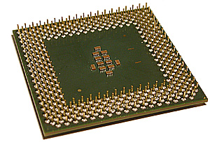
Intel Pentium
III 1.2GHz (click to enlarge)


